100W Darlington amplifikatör devresi

guclusat

Tanınmış Üye
Süper Moderatör
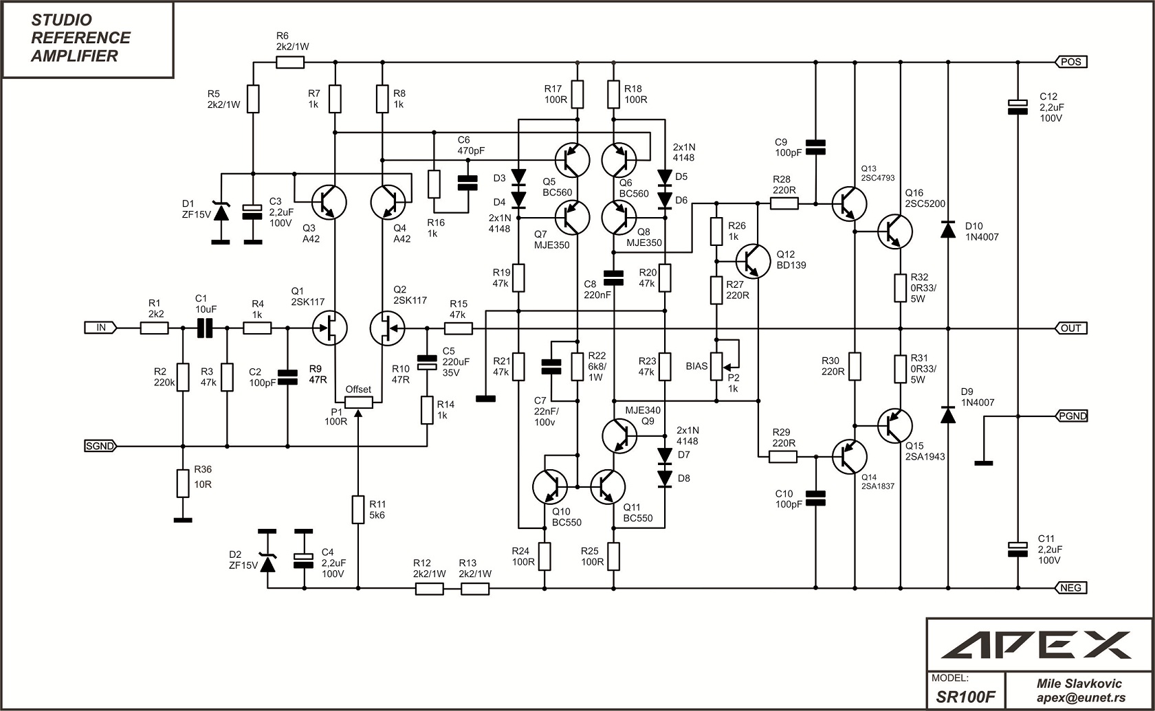
This design was intended for hi-fi use, or as a slave, bridging a gap between lower and higher power offerings, 'the need arose for an inexpensive, good quality, medium rated power amplifier design'. Design criteria were: must deliver 100W into 4 ohms, distortion must not exceed 0.1% at 100W (even at 20kHz), extensive power bandwidth, 'short-circuit proof', symmetrical supply negating use of output coupling capacitors, easy-to-obtain components, straightforward construction and calibration, should be economically viable and reliable.


elek100darl.gif

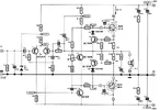
Relatively unsophisticated, with a low component count, the input was bootstrapped to increase the input impedance and current-limiting was included to supplement the fuses in the supply lines. Notable is the zener stabilised input 'tail', the class A driver being fed by the input transistor directly, the relatively low impedances of feedback network (and high value of DC blocking cap), 'tight' output transistor Vce of 100V, but conservatively rated mains transformer (mains filtering recommended).
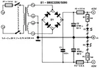
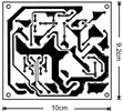
The bridge rectifier, smoothers, fuses and indicator LEDs were mounted on a separate PCB that sat below the amplifier PCB of the same size making a compact structure. Each output device had it's own SK84 1.2°C/W or SK03 100mm 1.8°C/W heat-sink. Adding a transformer then offered a complete and compact power amplifier solution.

Although no problems were encountered by the author and other constructors, compared to the later (December) Crescendo FET design which many thought unstable (two later versions of the Crescendo were published in May '84 - the 'Mini' and April '01 - the ME), the following mods were suggested by one builder to overcome the HF problems that he experienced;

"Reduce C6 to 27pf, and C7 and C8 to 10pF. Remove C1 and the current-limiting (T5, T6, D2, D3, R13, R15, R17 and R19). Parallel 0µ1F with D1 and 1µF (non-polarised) across bias transistor (T2, C to E). Replace C2 with 2µ2F (non-polarised) and fit a screen between the stackable PSU and PA PCBs."No thermal feedback for the bias was possible in the original, the bias transistor being mounted on the upper PCB, close to the input pair.
A variety of complementary Darlington pairs have been used in this design (the originals offering 150W, 100V, 3MHz, hFE 1,000). Lower power versions using MJ2501/3001 (150W, 80V, 1MHz, hFE 1,000 @ 5A) output devices have been seen, as have others with higher power stages using faster MJ11015/16s (200W, 120V, 2MHz, hFE 2,000 @ 20A). Versions with Rs 16-19 halved in value have appeared.

Additional components, intended to improve performance have been added to some builds.


elek100darlb.gif

A popular and easily upgraded design, sometimes described as 'winning' especially when compared in 'blind' tests with more complex circuits, that bears resemblances to older RCA designs. After more than 25 years versions are still being built, Velleman's (2008) K8060 amplifier (below), K8081 amplifier and K8077 sub-woofer kits all use designs which are a close match, less one resistor. Recommended heat-sink (for both output devices) 1.2°C/W.

vell100darl.gif

Looking at the respective RC networks, the original version offers a gain of 28.5 somewhere between 1.33Hz - 321kHz, whilst the much later Velleman gives a gain of 34 between 3.39Hz - 1.026MHz with half the quiescent current using higher gain (125W, 100V, hFE 3,000 @ 5A) output devices. Personal preference would retain the lower HF roll-over and increase the higher LF roll-off, ie; 10Hz - 300kHz. Additional bi-polar caps across the electrolytics, zener and bias transistor could improve, as can attention to the bias, as seen in the Velleman where the bias transistor is fitted to the heat-sink. Loading the base-emitters of the protection pair with capacitance will prevent triggering on permissible transients. No version seen has a thermally mated input pair.
 

Eklentiler

  • 100W Darlington amplifikatör devresi Uydudoktoru.zip
    587,4 KB · Görüntüleme: 317
Son düzenleme:
This is a nice final audio amplifier to build it and have fun. The amplifier is able to drive up to 100W to a 4 Ohm load or up to 70W to an 8 Ohm load. The total distortion is less than 0.1% (even in high frequencies). The circuit uses ordinary electronic components and the amplifier has DC coupled output, for best performance even at low frequencies.


The circuit

The final stage of the amplifier uses a pair of complementary Darlington transistors (T7 and T8). Darlington transistors offer high current and hence high power amplification.

The input stage uses T1 and T2. Then, there is a driving stage, which uses T3 and T4. T3 and T4 are connected in series. The driving stage is used for amplification but also to bias the final stage with a specific idle current.


The electronic circuit of the 100W audio amplifier
The final stage of the amplifier uses a symmetrical topology. A key advantage of the symmetrical topology is that the idle voltage on the load is zero. Therefore, there is no need for a DC blocking capacitor to isolate the load from any DC. Thus, by avoiding the use of a DC blocking capacitor, we also diminish any undesirable high pass filtering from an RC filter at the output (formed by the DC blocking capacitor and the load resistor).

The amplifier has high input impedance which is about 100K due a bootstrap biasing technique based on C4 and R2 and also, because T1, by its nature, has a quite high input impedance. T1 and T2 form a differential amplifier. A differential amplifier has two inputs: The first one is at the base of T1 and at the other one is at the base of T2. The first input receives the input signal directly, while the other input is used to add negative feedback from the output through R6. The feedback is DC coupled and the DC component of the feedback is used to stabilize the output to zero potential at rest.

The voltage gain (voltage amplification) of the differential input stage, which can be regarded as a non-inverting amplifier, is determined by the ratio of the sum R3 plus R6, to R3. That is:

Uo / Ui = (R3 + R6) / R3 = 1 + R6 / R3 = 3420/120 = 28,5

The base of T4 receives signal from the collector of T1. T4 and T3 amplify the input signal in order to provide enough power to drive the output stage. Due to the use of Darlington type transistors at the output, there is no need for extreme intermediate amplification. Due to this in fact, T4 and T3 do not use high currents and they do not get very hot, so they do not require do be cooled.

T3 biases the output stage and resistors R18 and R19 stabilize its operation. The idle DC voltage at the connection point of R18 and R19 (and moreover at the load) is adjusted from P1 potentiometer which actually adjusts the collector-emitter voltage of T3. R11 is "Bootstrapped" through C5, and its impedance is increased, thereby increasing the gain of the driver stage.

The output stage uses T7 and T8. T7 and T8 are complementary Darlington type transistors and they have the following characteristics (at room temperature):

  • maximum collector-emitter voltage = 100 V
  • maximum collector current = 16 A
  • maximum thermal loss = 150 W
No matter how efficient are the output transistors, we should protect them from overloading. For this reason we use T5 and T6.

The voltage drop across R18 or R19, is proportional to the output current. Thus, we use these voltages to sense a potential overload. In case of an overload (short circuit at the load), a high output current results in high voltage drops across R18 and R19. These voltages make T5 and T6 conductive via voltage dividers R16 / R14 and R17 / R15. At conductivity, T5 and T6 draw current from T7 and T8 bases, through D2 and D3, thereby limiting the driving current in T7 and T8.

All capacitors in the circuit have important roles:

C1 limits the frequency response at high frequencies above the audible range in order to limit the noise level. C3 is also used to cause attenuation at high frequencies. C6, C7 and C8, as well as R20 and C9, stabilize the amplifier. C10 and R21, C12, C11 and R22, serve to suppress any high frequency noise in the supply voltage.


Power supply

At peak output on a 4 Ohm load, the amplifier requires a current of about 2.25A. For an 8 Ohm load, the peak current is about 1.1 A. There is a common truth that the quality of an audio amplifier is strongly determined from its power supply unit. Indeed, that is true but there is no need for exaggerations. A simple power supply unit, able to provide symmetrical voltages of ± 40 V, is sufficient.

For low cost and simplicity, we use a simple non- stabilized power supply unit. Given the absence of stabilization, output voltages of ± 40 V correspond to a low limit, during peak power consumption. At less than peak power, the power consumption is reduced, and the output voltage of the non stabilized power supply unit is expected to be higher than 40V.


2x45V power supply circuit
However, the transistors of the amplifier withstand up to a maximum of ± 50 V. Therefore, to ensure a safety margin, we prefer to build a power supply unit at ± 46 V. Thus, we expect to have a small difference of about 6 V, between resting and full load. This is a quite small voltage drop which requires a very low internal resistance of the power supply unit. The internal resistance of a non stabilized power supply unit is mostly determined by the transformer. That's why we prefer to use a high quality toroidal transformer.

The power supply unit has only a transformer, a diodes bridge rectifier and some electrolytic capacitors for voltage smoothing. Fuses are also used for protection in case of a permanent short circuit.

The 100W audio amplifier circuit can be used for a single audio channel. Therefore, if you want to create a stereo version of the amplifier, you may use two identical circuits and two identical power supply units.


Some construction details

The amplifier and the power supply can be easily built in the printed circuit boards provided herein:


The printed circuit board of the 100W audio amplifier
It is a good practice for the power resistors R18 and R19, to be placed at a distance of at least 5 mm from the circuit board surface. This way, we ensure good air flow for sufficient heat diffuse.

Sufficient heat sinks are required for T7 and T8. It is better to place T7 and T8 on separate heat sinks of 1.2 ° C / W. If you put the two transistors on the same heat sink, then you need to divide the thermal resistance of the heat sink with the total number of the transistors. Therefore, for the two transistors (T7 and T8) on the same heat sink, a thermal resistance less than or equal to 0.6 ° C / W would be sufficient.


The printed circuit board for the 2x45V power supply unit
There should be no direct contact between any transistor and the heat sink. Unexpected short-circuits may arise from direct contact (for example, if the heat sink is mounted to a grounded chassis, or both transistors are placed on the same heat sink) and that is because the metallic case of each transistor is internally connected to the collector). Thus, for mounting the transistors on their heat sink(s), you may use appropriate insulators, e.g. of mica.


How to assemble the amplifier
You must use a suitable shielded cable for the input signal and cable’s shield should be grounded.

The boards of both the amplifier and the power supply have exactly the same dimensions. This is done intentionally, in order to allow the mounting of the power supply board directly below the amplifier’s board by using screws and spacers. This "intelligent" arrangement reduces the required space and allows the construction of an autonomous module.


How to assemble the 2x45Vpower supply unit

Initial calibration


After construction, the amplifier requires some calibration. The calibration is a simple adjustment of P1 trimmer.

The calibration is done with the aim of a DC ampere meter – millimeter while setting a zero input signal. During calibration, the load (speaker) should be also disconnected..

Calibration steps:

Turn off power supply. Short-circuit the input of the amplifier to ensure the absence of an input signal. Make sure that the output is not connected anywhere (disconnect any speaker).

Remove F2 fuse and place the terminals of an ammeter at its terminals. The ammeter should be set at a 1A DC scale.

Turn P1 potentiometer fully anticlockwise. Check all connections and connect power supply. The ammeter should show approximately 0A. If the reading is greater than zero, immediately disconnect power supply and check for any circuit error.

If everything is as it should be, change the scale of the ammeter to 100mA and adjust P1 so that the milli-ammeter to show approximately 80mA. At that time, the quiescent current in the output transistor will be about 50mA.

Calibration completed. Place F2 fuse at its place and enjoy.

If someone goes wrong, don’t be upset. Just find the error by taking voltage at current measurements at some circuit nodes and compare these measurements with reference values indicated at the schematic. Reference values have been measured while the load (speaker) was connected, and there was a zero input signal.

audio_amplifier_photo_1.JPG

100W audio amplifier

List of components (100W amplifier)

Resistors (1/4W or 1/2W unless otherwise noted):

R1 = 120K

R2, R5, R6 = 3K3, R3 = 120Ω

R4, R8 = 680Ω, R7 = 1K5

R9 = 5K6, R10 = 1K2, R11 = 2K7

R12, R13 = 270Ω, R14, R15 = 15Ω, R16, R17 = 220Ω, R18, R19 = 1Ω/9W, R20 = 10Ω

R21, R22 = 1Ω, P1=trimmer pot 1K

Capacitors :

C1 = 470pF

C2 = 10µF/63V, C3 = 150pF

C4 = 1000µF/10V, C5 = 220µF/50V, C6 = 47pF

C7, C8 = 560pF, C9 = 47nF

C10, C11 = 680nF, C12, C13 = 100nF

Semiconductors :

T1, T2 = BC 556A, T3, T5 = BC 547B, T4 = BC 639

T6 = BC 557B

T7 = BDX67B or BDX67C, T8 = BDX66B or BDX66C, D1 =zener 9V1/1.3W

D2, D3 = 1N4148 or 1N914


List of components (2x45V power supply unit)

Resistors:

R1, R2 = 3K3/1W

Capacitors:

C1 = 100nF

C2, C3 = 4700µF/63V

Semiconductors : D1, D2 = LED

B1 = B80 C3200/5000 diodes rectifier bridge

Rest:

F1 = fuse 1,5A

F2, F3 = fuses 2,5A

Tr1 = Transformer 2x30V, 2x3.75A or more, 225VA or more
 

Eklentiler

  • power_supply_2x45V_assembly.jpg
    power_supply_2x45V_assembly.jpg
    57 KB · Görüntüleme: 53
  • audio_amplifier_100W_schematic.jpg
    audio_amplifier_100W_schematic.jpg
    73,5 KB · Görüntüleme: 53
  • power_supply_2x45V.jpg
    power_supply_2x45V.jpg
    28,7 KB · Görüntüleme: 48
  • audio_amplifier_100W_pcb.jpg
    audio_amplifier_100W_pcb.jpg
    61,1 KB · Görüntüleme: 51
  • power_supply_2x45V_pcb.jpg
    power_supply_2x45V_pcb.jpg
    39,3 KB · Görüntüleme: 53
  • audio_amplifier_100W_assembly.jpg
    audio_amplifier_100W_assembly.jpg
    59,1 KB · Görüntüleme: 57

APEX SR100F AMPLİFİKATÖR Devresi

Transistörler:

- Q1, Q2 - 2SK117 - 2 adet.
- Q3, Q4 - MPSA42 - 2 adet.
- Q5, Q6 - BC560 - 2 adet
- Q7, Q8 - MJE350 (KSE350) - 2 adet.
- S9 - MJE340 (KSE340) - 1 adet.
- Q10, Q11 - BC550 - 2 adet
- S12 - BD139 (MJE340) - 1 adet.
- S13 - 2SC4793 - 1 adet.
- S14 - 2SA1837 - 1 adet.
- S16 - 2SC5200 - 1 adet.
- S17 - 2SA1943 - 1 adet.

Diyotlar, zener diyotları:

- D1, D2 - ZF15V (zener diyotları 15 Volt) - 2 adet.
- D3, D4, D5, D6, D7, D8 - 1N4148 - 6 adet.
- D9, D10 - 1N4007 - 2 adet

Dirençler:

- R1 - 2k2 - 1 adet.
- R2 - 220k - 1 adet.
- R3, R15, R19, R20, R21, R23 - 47k - 6 adet
- R4, R7, R8, R14, R16, R26 - 1k - 6 adet
- R5, R6, R12, R13 - 2k2 / 1W - 4 adet (iki 3k3 / 2W direnç kart üzerine monte edilmiştir)
- R9, R10 - 47R - bunların yerine 100R dereceli bir düzeltici DC OFSET rezistörü monte edilmiştir - 1 adet.
- R11 - 5k6 - 1 adet.
- R17, R18, R24, R25 - 100R - 4 adet
- R22 - 6k8 / 1W - 1 adet.
- R27, R28, R29, R30 - 220R - 4 adet.
- R31, R32 - 0R33 / 5W - 2 adet.
- R36 - 10R / 1W - 1 adet.
- P1 - ayar direnci DC OFSET - 100R - 1 adet.
- P2 - ayar direnci BIAS - 1 ... 1,5k - 1 adet.

Kondansatörler:

- C1 - 10mF / 63V film - 1 adet.
- C2, C9, C10 - 100p seramik - 3 in /
- C3, C4, C11, C12 - 2.2mF / 100V elektrolit - 4 adet.
- C5 - 220mF / 35V elektrolit - 1 adet.
- C6 - 470p - 1 adet.
- C7 - 22n / 100V - 1 adet.
- C8 - 220n - 1 adet.
 

Eklentiler

  • 100W_amp_devresi.zip
    1,4 MB · Görüntüleme: 172
Amplifikatör elemanlarının listesi:

Entegre :
- NE5532 - 1 adet.
- IR2117 - 2 adet.

Transistörler:

- 2N5401 - 2 adet.
- 2N5551 - 1 adet.
- MJE340 - 2 adet.
- MJE350 - 1 adet.
- MJE15032 - 1 adet.
- MJE15033 - 1 adet.
- 2SC5200 - 4 adet.
- 2SA1943 - 4 adet.
- IRF540 - 4 adet.
- BF421 - 1 adet.

Zener diyotlar:

- 1N4007 - 3 adet.
- ZY15V - 9 adet
- 1N4148 - 6 adet.
- BAV21 - 3 adet.
- SFA1603 - 2 adet.
- LDR - NSL32 - 1 adet.

Rezistörler:

- 3k3 - 1 adet.
- 10k - 3 adet.
- 33k - 1 adet.
- 43k - 1 adet.
- 4k7 - 6 adet
- 6k8 / 2W - 1 adet.
- 47k - 1 adet.
- 2k2 / 2W - 2 adet
- 22k - 4 adet.
- 1k - 3 adet.
- 1k5 - 2 adet.
- 100R - 2 adet.
- 680R - 1 adet.
- 330R - 1 adet.
- 4R7 / 2W - 5 adet.
- 390R - 4 adet.
- 56k - 3 adet.
- 150k - 2 adet.
- 22k / 1W - 2 adet.
- 3k3 / 1W - 2 adet.
- 100k - 2 adet.
- 5k6 - 1 adet.
- 22R - 1 adet.
- 0R33 / 5W - 8 adet.

Kondansatörler:

- 22mF / 25V - 3 adet.
- 33p - 1 adet.
- 2,2mF / 25V - 2 adet.
- 100n - 4 adet
- 47mF / 25V - 2 adet.
- 470p - 1 adet.
- 47n / 100V - 5 adet.
- 100p - 2 adet.
- 22p - 1 adet.
- 150p - 2 adet.
- 10mF / 160V - 2 adet.
- 100mF / 25V - 5 adet.
- 10mF / 63V - 1 adet.

Gerisi:

- Tahta üzerine montaj için sigorta bloğu - 2 adet.
- Sigorta 15A - 2 adet.
- Prizler 8 Pimli - 3 adet.
- Konektör 2 Pim 5 mm - 3 adet.

Sonuç olarak iki yükseltici kanalın köprü köprüsünü vereceğim (Köprü):


Eklentiler

  • H900_Anfi_devresi.zip
    3,1 MB · Görüntüleme: 161
Geri
Yukarı