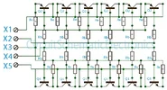
This power amplifier driver is a very powerful power driver called Namec TEF, Namec itself stands for New American Driver power amplifier is very suitable to use sanken Final 2sc2922 2sa1216 transistors, Power output can produce up to 1000W. To assemble this power amplifier is bothered easy, very simple schematics and components. but need carefulness and diligence in assembling this power. See below the circuit schematic of Driver Power Amplifier Namec TEF:

Part List:
Resistor
R1=4k7
R2=47k
R3=4k7
R4=12k
R5=330R
R6=47k
R7=22k
R8=33k
R9=100R/2W
R10=47k
R11=2k2
R12=1k
R13=10R
R14=100R/2W
R15=1k5
R16=220R
R17=150R/2W
R18=150R/2W
R19=56R/2W
R20=56R/2W
RV1=1K Trimpot
RV2=1K Trimpot
Capacitor
C1=4u7/50V
C2=100pF
C3=47u/100V
C4=100u/100V
C5=100N
C6=100u/100V
C7=100N
Diode
D1= ZD12V/1W
Transistor
Q1=C945
Q2=TIP42
Q3=C945
Q4=TIP41
Q5=MJE340
Q6=TIP42
Q7=TIP41
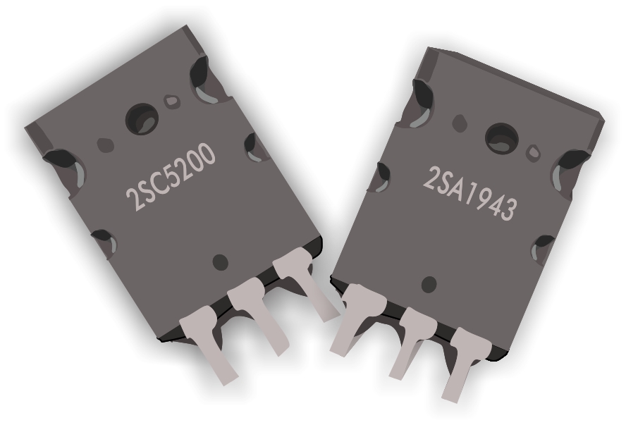
Q8=2SA1943
Q9=2SC5200
Connector
J1=Audio Input
J2= To (-) Base Final Transistor
J3= To (+) Base Final Transistor
J4= VCC+ 45V - 80V DC
J5=VCC- 45V - 80V DC
GND= Ground
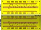
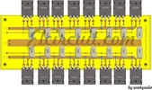
To make it easy assembling the driver power amplifier you can make with this PCB Layout design below:

.webp")
Part List:
Resistor
R1=4k7
R2=47k
R3=4k7
R4=12k
R5=330R
R6=47k
R7=22k
R8=33k
R9=100R/2W
R10=47k
R11=2k2
R12=1k
R13=10R
R14=100R/2W
R15=1k5
R16=220R
R17=150R/2W
R18=150R/2W
R19=56R/2W
R20=56R/2W
RV1=1K Trimpot
RV2=1K Trimpot
Capacitor
C1=4u7/50V
C2=100pF
C3=47u/100V
C4=100u/100V
C5=100N
C6=100u/100V
C7=100N
Diode
D1= ZD12V/1W
Transistor
Q1=C945
Q2=TIP42
Q3=C945
Q4=TIP41
Q5=MJE340
Q6=TIP42
Q7=TIP41
Q8=2SA1943
Q9=2SC5200
Connector
J1=Audio Input
J2= To (-) Base Final Transistor
J3= To (+) Base Final Transistor
J4= VCC+ 45V - 80V DC
J5=VCC- 45V - 80V DC
GND= Ground
To make it easy assembling the driver power amplifier you can make with this PCB Layout design below:
Son düzenleme: