
Güncel olmayan bir tarayıcı kullanıyorsunuz. Bunu veya diğer web sitelerini doğru şekilde görüntülemeyebilir.
Yeni sürüme geçmeli veya bir alternatif kullanmalısınız. tarayıcı.
Yeni sürüme geçmeli veya bir alternatif kullanmalısınız. tarayıcı.
Frekansı Voltaja çeviren devre şemaları


Databilgilerinden bir devre şeması
TC9400 Voltage to Frequency converter (Single supply version)
In the circuit shown above the TC9400 is wired as a F to V converter that operates from a single supply. The circuit generates an output voltage that is proportional to the input frequency. The input frequency is applied to the pin11 (non inverting input of the internal comparator). In order to trip the comparator the amplitude of the input frequency must be greater than +/-200mV.Below this level the circuit will not work at any situation.
Whenever the input signal to the pin 11 of IC1 crosses zero to the negative direction the output of the internal comparator goes low. The 3uS delay circuit enables the Cref charge/discharge circuit after 3uS and this connects the Cref to the reference voltage and this charges the integrating capacitor Cint a specific amount of voltage. In the single supply operation the reference voltage is the potential difference between pin 2 and 7 of the TC9400. Each time the input frequency wave form crosses zero towards positive direction, the output of the internal comparator goes high and this disables the Cref charge/discharge circuit which creates a short circuit across the Cref leads. The voltage across the integrating capacitor Cint is retained because the only discharge path available is the 1M resistor Rint which is a too high and the voltage across Cint is the output voltage. Resistor Rbiasis used to set the bias current of the IC.
The potential divider network comprising of R6 and R7 makes sure that the input threshold tracks the supply voltage always. The clamp circuit using diode D2 prevents the input from going far negative in order to turn on the internal comparator. In simple words this section of the circuit can be generally termed as a level shifter.
The TC9400 manufacturers claim that it can accept a signal of any frequency at its input. In the practical side, for the proper working of this circuit the positive half of the input signal must have at least 5uS pulse width and for the negative half it must be greater than or equal to 5uS.
For calibration adjust the offset adjust trimpot to obtain 0V at the output with no input frequency applied. If you have a function generator, set frequency input to 10KHz and make adjustments in the value of Cref to get around 2.5 to 3 volts at the output. This calibration is meant for a maximum input frequency of 10KHz.
Notes.
- The circuit can be assembled on a Perf board or PCB.
- The circuit can be powered from anything between 10 to 15V DC.
- R3 can be used for adjusting the offset voltage.
- In the circuit the inverting input of the internal comparator is referenced to 6.2V by using D1. So the input signals amplitude must be between 4V and the supply voltage (V+).
- The output voltage is also referenced to 6.2V in this circuit.
- The output voltage and input frequency of the F to V converter is related using the equation V out = V ref x C ref x F in where V out is the output voltage and F in is the input frequency.
- TC9400 and TL071 must be mounted on holders.
Son düzenleme:

Frequency to Voltage Converter Circuit,

Required Material
Required Material
- KA331 IC - 1pc
- .01uF ceramic capacitor - 1pc
- 470pF ceramic capacitor - 1pc
- 1uF Electrolytic capacitor with a 16V rating
- 10k resistor with 1% stability rating MFR - 2pcs
- 100k resistor with 1% stability rating MFR - 2pcs
- A 68k resistor with 1% stability rating MFR - 1pc
- A 6.8k resistor with 1% stability rating MFR - 1pc
- Breadboard
- 15V power supply
- Single strand wire
- A frequency generator or function generator to check the overall circuit.


My Electronics LAB
Gold Member
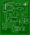
XR4151 entegresiyle yapılan, frekans voltaj dönüştürücü devresidir. Bu devreyle alakalı baskı devre ve lay dosyası ektedir. Bunun gibi bu tarz devreler, iyi bir bitirme ödevi veya tezi olabilir. Bu konuya hakim ilgi alaka duyan herkese faydalı olabilir.
Eklentiler
Voltage To Frequency

The LM331 is a very linear, temperature-compensated voltage to frequency converter, which is normally used in circuits where 0 volts gives 0 hertz. To allow bipolar operation, a constant voltage must be added to the input voltage to provide a bias. It's important that this bias voltage also be temperature compensated, but fortunately the LM331 happens to have just such a voltage available at pin 2 as part of its frequency sensitivity adjustment.
The LM331 supplies a constant, temperature-compensated 1.90 V at pin 2, across R4. The current through R4 affects the output frequency, so an LF351 op-amp buffer is used to obtain a solid copy of this voltage without drawing significant current.
That constant voltage is then summed with the input voltage via R7, R1, and R8, where its relative contribution is controlled by R7 to provide the effective bias voltage.
The LF351 is powered between the +9 V battery supply and ground, even though it is not a single-supply op-amp. That doesn't matter here because all pins are always at 1.90 V above the "negative" supply pin 4. (You can substitute a TL081 or other low bias current JFET-input amp here.)
To change the voltage range, you only need to change R4 and R7. The complete equations below are based upon the LM331 datasheet, which says that for a given voltage V7 at pin 7 the output frequency F is:
F = V7 * R4 / N
Where N = (2.09 * R3 * R2 * C2)
For R3 = 100K, R2 = 6.8K and C2 = 0.01 microfarad, we find N = 14.212.
But the R1, R7, R8 summing network affects the V7 voltage. We will assume that R1 = R8 and solve for R7, where we specify the output frequency F0 for an input of 0 V, and Fp for the full-scale positive input voltage Vp.
Note that this also assumes that F0 is big enough to allow a full-scale negative swing below it. If the positive range and negative range are to be equal, then the frequency Fn for a full-scale negative input will be:
Fn = 2 * Fp - F0
Fp and F0 must be chosen so that Fn is above zero, preferably at least 100 Hz or so. Other than that, we can ignore Fn for the rest of the calculations. Omitting a lot of tedious algebra, we find:
R7 = (Fp - F0) * 1.9 * R1 / F0 * Vp
and
R4 = N * F0 * (2 * R4 + R1) / (1.9 * R1)
For F0 = 1500, Fp = 2000, Vp = 5 V, and R1 = R8 = 100K, we get:
R7 = (2000 - 1500) * 1.9 * 100K / 1500 * 5 = 12.667K
R4 = 14.212 * 1500 * (2 * 12.667K + 100K) / 1.9 * 100K = 14.062K
To change the input voltage range from +/-5 to +/-1 while keeping the same output frequency range, we get R7 = 63.333K and R4 = 25.432K.
Note that the output is a stream of rectangular high-to-low pulses. The pulse width T is given by:
T = 1.1 * R2 * C2
For the R2 and C2 values given, this is about 75 microseconds. The maximum frequency of operation is limited to a period of about twice this, or 1 / 150 microseconds = 6.7 kHz.
The above schematic plus complete 600 DPI board and parts placement layouts suitable for printing are included in the VoltToFreqAll600.PNG file that is installed with Daqarta in the Documents - Daqarta - Circuits folder.
Be sure to read the Notes section of Daqarta Printed Circuits before you begin.
You can use the printed layouts directly to create your own circuit boards, with either the laser printer toner transfer method, or with the direct-draw method discussed under Printed Circuit Construction.
Alternatively, you can edit the VoltToFreq.PCB file in the same folder to make custom modifications first. See the PCB Files discussion in Daqarta Printed Circuits for the required software to use this file, and for information on how to submit it to have boards made by a 3rd-party supplier.
Note that in the component placement layout the total R4 value is shown as series resistors R4A and R4B. This allows you to combine values to get closer to the computed value for R4, in case you want to use this same circuit in some other context. (In that case, you may want to edit the PCB file to allow R7 to be made up of 2 series values as well.)
In Daqarta, however, the Fcal High and Low controls make these series values completely superfluous; you can use any single value that is reasonably close. If you bend the R4 resistor so that the leads are 0.5 inch apart instead of the standard 0.4 inch, you can insert it just below the R4A position and it will reach ground without needing a separate jumper.


This voltage to frequency converter circuit has an oscillator that is voltage controlled and has a small, 0.5% deviation. IC1 function as a multivibrator and produces rectangular impulses with equal width.
The width of the impulses depend on R4, P1 and C1. With P1 we can do fine adjustments of the output frequency.
The output frequency can be easily adjusted with the help of U1 voltage. D3 diode is required because we want to eliminate R4 and P1 influence. D1 and D2 diodes produce a small flow of temperature. With P2 we adjust the offset voltage. Because of its high quality, this voltage-frequency converter (VCO) can be used in a large field of applications.
FREKANS-VOLTAJ dönüştürücü devresi
Amatör radyo devrelerinde, örneğin frekansı bir voltmetre (multimetre), frekans değişikliklerine tepki veren bir sensör vb. ile ölçmek için frekans-voltaj dönüşümüne ihtiyaç vardır.Bu durumda, frekansı voltaja dönüştürmek için LM331 mikro devresi kullanılır. Giriş darbeleri dikdörtgen olmalıdır, blokaj kapasitörü C1 üzerinden LM331'in IC1 girişine (pim 6) beslenirler. Bu pim, direnç R7 üzerinden bir artı ile aralıklıdır.
R2 ve R3 dirençleri arasındaki bölücü, pim 7'deki voltaj seviyesini ayarlar - maksimum çıkış voltajı. R3 direncinin değeri aşağıdaki formüle göre seçilir: R3 = (Vcc - 2V) / 1.9, burada Vcc besleme voltajıdır ve R3 kilo-ohm olarak ifade edilir.

LM331 mikro devresindeki frekans-voltaj dönüştürücünün şematik diyagramı
Çıkış voltajı (V çıkışı) aşağıdaki formül kullanılarak hesaplanır:Uout = ((R4 / (R5 + R6)) x R1 x C1 x 2.09 x Fin.
Çıkış voltajını ayarlamak için düzeltici direnç R6 kullanılabilir. Dönüştürücü frekans aralığında çalışır: 10Hz - 5 kHz; çıkış voltajı değişir: 0.025 ila 12.5V.
R3 değeri, depolama voltajına ve R3 = (Vs - 2V) / (2mA) tasarımına bağlıdır. Vs = 15V - R3 = 68k için
IC LM331, 5 ila 30VDC arasında çalışabilir.
Potansiyometre R6, dönüştürme devresini kalibre etmek için kullanılabilir.
Bu şemaya dayanarak, salon sensöründen gelen darbeleri sayacak bir araba (motosiklet ...) için elektronik bir takometre monte edebilirsiniz. Çıkışa bir analog veya dijital voltmetre bağlanabilir.
