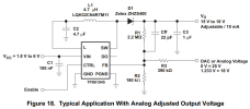
The TPS61045 is a high frequency boost converter with digitally programmable output voltage and true shutdown. During shutdown, the output is disconnected from the input by opening the internal input switch. This allows a controlled power up/down sequencing of the display. The output voltage can be increased or decreased in digital steps by applying a logic signal to the CTRL pin. The output voltage range, as well as the output voltage step size, can be programmed with the feedback divider network. With a high switching frequency of up to 1 MHz, the TPS61045 allows the use of small external components and together, with the small 8-pin QFN package, a minimum system solution size is achieved.
DAC = 1.233V : V0 = 1.233 * ( 1 + 2200/180 ) = 16.303V
SETTING THE OUTPUT VOLTAGE (see Figure 1)
When the converter is programmed to the minimum output voltage,
the DAC output (DO) equals the reference voltage of 1.233 V (typ).
Therefore, only the feedback resistor network (R1) and (R2) determines the output voltage under these conditions.
This gives the minimum output voltage possible and can be calculated as:
The maximum output voltage is determined as the DAC output (DO) is set to 0 V:
the DAC output DO (pin 3) one-step where one step is typically 19.6 mV. ( 0..63 : 6 Bit DAC )
The DAC output pin (DO) drives an external resistor (R3) connected to the external feedback
divider. The DO output has a typical output voltage range from 0 V to Vref (1.233V). If the DO output voltage is
set to 0 V, the external resistor (R3) is more or less in parallel to the lower feedback resistor (R2) giving the
highest output voltage. Programming the DO output to Vref gives the lowest output voltage. Internally, a 6-bit DAC
is used with 64-steps and 0 as the first step. This gives a typical voltage step of 19.6 mV which is calculated as:
A voltage step on DO of 19.6mV (typ) changes the output voltage by one step and is calculated as:
The possible output voltage range is determined by selecting R1, R2 and R3.
A possible larger output voltage range gives a larger output voltage step size.
The smaller the possible output voltage range, the smaller the output voltage step size.
DIGITAL INTERFACE (CTRL)
When the CTRL pin is pulled high the device starts up with softstart
and the DAC output voltage (DO) sets to its center voltage with a typical output voltage of 607 mV.
The output voltage can be programmed by pulling the CTRL pin low for a certain period of time.
Depending on this time period the internal DAC voltage increases or decreases one digital step,
as outlined in Table 2 and Figure 16.
Programming the DAC output V(DO) to 0 V places R3 in parallel to R2, which gives the maximum output voltage.
If the DAC is programmed to its maximum output voltage equal to the internal reference voltage, typically V(DO) = 1.233 V,
then the output has its minimum output voltage.
- Input Voltage Range . . .1.8 V to 6 V
- Output voltage of up to 28V possible
- Up to 85% Efficiency
- Digitally Adjustable Output Voltage Control
- Disconnects Output From Input During Shutdown
- Switching Frequency . . . Up to 1 MHz
- No Load Quiescent Current . . . 40 µA Typ
- Thermal Shutdown Mode
- Shutdown Current . . . 0.1 µA Typ
- Available in Small 3mm × 3mm QFN package
- APPLICATIONS
DAC = 1.233V : V0 = 1.233 * ( 1 + 2200/180 ) = 16.303V
SETTING THE OUTPUT VOLTAGE (see Figure 1)
When the converter is programmed to the minimum output voltage,
the DAC output (DO) equals the reference voltage of 1.233 V (typ).
Therefore, only the feedback resistor network (R1) and (R2) determines the output voltage under these conditions.
This gives the minimum output voltage possible and can be calculated as:
The maximum output voltage is determined as the DAC output (DO) is set to 0 V:
the DAC output DO (pin 3) one-step where one step is typically 19.6 mV. ( 0..63 : 6 Bit DAC )
The DAC output pin (DO) drives an external resistor (R3) connected to the external feedback
divider. The DO output has a typical output voltage range from 0 V to Vref (1.233V). If the DO output voltage is
set to 0 V, the external resistor (R3) is more or less in parallel to the lower feedback resistor (R2) giving the
highest output voltage. Programming the DO output to Vref gives the lowest output voltage. Internally, a 6-bit DAC
is used with 64-steps and 0 as the first step. This gives a typical voltage step of 19.6 mV which is calculated as:
A voltage step on DO of 19.6mV (typ) changes the output voltage by one step and is calculated as:
The possible output voltage range is determined by selecting R1, R2 and R3.
A possible larger output voltage range gives a larger output voltage step size.
The smaller the possible output voltage range, the smaller the output voltage step size.
DIGITAL INTERFACE (CTRL)
When the CTRL pin is pulled high the device starts up with softstart
and the DAC output voltage (DO) sets to its center voltage with a typical output voltage of 607 mV.
The output voltage can be programmed by pulling the CTRL pin low for a certain period of time.
Depending on this time period the internal DAC voltage increases or decreases one digital step,
as outlined in Table 2 and Figure 16.
Programming the DAC output V(DO) to 0 V places R3 in parallel to R2, which gives the maximum output voltage.
If the DAC is programmed to its maximum output voltage equal to the internal reference voltage, typically V(DO) = 1.233 V,
then the output has its minimum output voltage.
Eklentiler
Son düzenleme:

