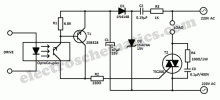
This universal triac controller circuit with optocoupler solves the problem that triacs have when functioning at low temperatures (triac needs higher gate current) by adding a transistor at the output of the optocoupler circuit.
The transistor amplifiers the trigger pulse coming from the optocoupler and the gate current is high enough to trigger the triac in all temperature cases.
How does the circuits works?
The base of the transistor is driven by the OC. C2 works as capacitive bias resistance to avoid power losses and it also helps avoid DC loading of the supply line. The switch current is limited by R3. D1 works as one-way rectifier while C1 works as ripple filter.
D2 stabilize the rectified voltage to 15 V.
T1 conducts when the OC sends a pulse to its base. C discharges through the collector-emitter line. The trigger current is limited by R2 to around 40 mA.
The discharge current time of C1 is less than 1 ms.
The RC circuit R4 and C3 protects the triac from voltage spikes.
This is very important in all inductive loads.
Triac Optocoupler Controller Schematic

Son düzenleme:
