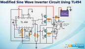
A very simple yet highly sophisticated modified sine wave inverter circuit is presented in the following post. The use of the PWM IC TL494 not only makes the design extremely economical with its parts count but also highly efficient and accurate.
Using TL494 for the Design
The IC TL494 is a specialized PWM IC and is designed ideally to suit all types of circuits which require precise PWM based outputs.
The chip has all the required features in-built for generating accurate PWMs which become customizable as per the users application specs.
Here we discuss a versatile PWM based modified sine wave inverter circuit which incorporates the IC TL494 for the required advanced PWM processing.
Referring to the figure above, the various pinout functions of the IC for implementing the PWM inverter operations may be understood with the following points:
Pinout Function of the IC TL494
Pin#10 and pin#9 are the two outputs of the IC which are arranged to work in tandem or in a totem pole configuration, meaning both the pinouts will never become positive together rather will oscillate alternately from positive to zero voltage, that is when pin#10 is positive, pin#9 will read zero volts and vice versa.
The IC is enabled to produce the above totem pole output by linking pin#13 with pin#14 which is the reference voltage output pin of the IC set at +5V.
Thus as long as pin#13 is rigged with this +5V reference it allows the IC to produce alternately switching outputs, however if pin#13 is grounded the outputs of the IC is forced to switch in a parallel mode (single ended mode), meaning both the outputs pin10/9 will begin switching together and not alternately.
Pin12 of the IC is the supply pin of the IC which can be seen connected to the battery via a dropping 10 ohm resistors which filters out any possible spike or a switch ON surge for the IC.
Pin#7 is the main ground of the IC while pin#4 and pin#16 are grounded for some specified purposes.
Pin#4 is the DTC or the dead time control pinout of the IC which determines the dead time or the gap between the switch ON periods of the two outputs of the IC.
By default it must be connected to ground so that the IC generates a minimum period for the "dead time", however for achieving higher dead time periods, this pinout can be supplied with an external varying voltage from 0 to 3.3V which allows a linearly controllable dead time from 0 to 100%.
Pin#5 and pin#6 are the frequency pinouts of the IC which must be connected with an external Rt, Ct (resistor, capacitor) network for setting up the required frequency across the output pinouts of the IC.
Either of the two can be altered for adjusting the required frequency, in the proposed PWM modified inverter circuit we employ a variable resistor for enabling the same. It may be adjusted for achieving a 50Hz or 60Hz frequency on pins9/10 of the IC as per the requirements, by the user.
The IC TL 494 features a twin opamp network internally set as error amplifiers, which are positioned to correct and dimension the output switching duty cycles or the PWMs as per the application specs, such that the output produces accurate PWMs and ensures a perfect RMS customization for the output stage.
Error Amplifier Function
The inputs of the error amplifiers are configured across pin15 and pin16 for one of the error amps and pin1 and pin2 for the second error amplifier.
Normally only one error amplifier is used for the featured automatic PWM setting, and the other error amp is kept dormant.
As can be seen in the diagram, the error amp with the inputs at pin15 and pin16 is rendered inactive by grounding the non-inverting pin16 and by connecting the inverting pin15 to +5V with pin14.
So internally the error amp associated with the above pins remain inactive.
However, the error amp having the pin1 and pin2 as the inputs are effectively used here for the PWM correction implementation.
The figure shows that pin1 which is the non-inverting input of the error amp is connected to the 5V reference pin#14, via an adjustable potential divider using a pot.
The inverting input is connected with pin3 (feedback pin) of the IC which is actually the output of the error amps, and enables a feedback loop to form for pin1 of the IC.
The above pin1/2/3 configuration allows the output PWMs to be set accurately by adjusting the pin#1 pot.
This concludes the main pinout implementation n guide for the discussed modified sine wave inverter using the IC TL494.
Output Power Stage of the Inverter
Now for the output power stage we can visualize a couple of mosfets being used, driven by a buffer BJT push pull stage.
The BJT stage ensures ideal switching platform for the mosfets by providing the mosfets with minimum stray inductance issues and quick discharge of the internal capacitance of the fets. The series gate resistors prevent any transients trying to make its way into the fet thus ensuring the operations to be entirely safe and efficient.
The mosfet drains are connected with a power transformer which could be an ordinary iron cored transformer having a primary configuration of 9-0-9V if the inverter battery is rated at 12V, and the secondary could be 220V or 120V as per the user's country specs.
The power of the inverter is basically determined by the transformer wattage and the battery AH capacity, one can alter these parameters as per individual choice.
Using Ferrite Transformer
For making a compact PWM sine wave inverter, the iron core transformer can be replaced with a ferrite core transformer. The winding details for the same may be seen below:
By using super enamelled copper wire:
Primary: Wind 5 x 5 turns center tap, using 4 mm (two 2 mm strands wound in parallel)
Secondary: Wind 200 to 300 turns of 0.5 mm
Core: any suitable EE core which would be capable of accommodating these winding comfortably.

Son düzenleme:
