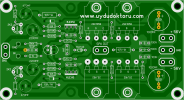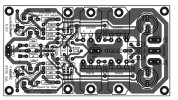
MOSFET Integrated Amp Power Amplifier
This circuit is from David White's article in Electronics World (August 2001). It uses inexpensive HexFet™ Power MOSFETs as output devices. Since their transconductance is low, the rest of the design is geared towards producing maximum open-loop gain. Overall Negative Feedback is used to set the gain to 27dB and to reduce the distortion.
The input devices used (2SA970) are low-noise, high gain PNP devices. They have poor Vce(max), so their supply voltage is reduced using a simple Zener diode regulator built using R3, ZD1 and C3. T1 is used as a current source. The author of the original EW article mentioned using a plain gate-source connected JFET, which is selected to produce 1mA current. At Rs. 25 a pop, I was not about to do this with BF245s. Besides, the current for my G-S connected BF245s is around 7mA. Insert a resistance in series with the source to reduce the current. Since the source-drain current is dependent on the manufacturing process, you should select the resistor for each BF245 in a multiple-amp. system. The value should be selected for 1mA current. If required, use a 1k pot here.
C1 forms the input blocking cap, but is shorted with a jumper because the blocking capacitor is already present on the preamp board. R1 and R2, together with C2 form an RF suppression network at the input. R2 sets the input impedance at 47kΩ. R4 and R5 are the collector loads for T2 and T3. I found that using a current mirror did not improve the THD rating of the amp (at least in Spice), so I dropped that idea. ZD2 (A 2.7V Zener), C4 and C5 prevent the base of T4 from getting beyond 2.7V in the event of amplifier clipping, output device failure, etc.
T9 and T10 forms the voltage amplifer stage (VAS). The original circuit recommended using 2SD756 transistors, which I couldn't find. The BF420 is similar, with slightly lower beta. It's a differential stage, with a constant current source formed by T6, T7, LD1, LD2, R10 and R11. A Wilson current mirror, formed by T4, T5, D1, R8 and R9 acts as the collector load for T9 and T10, ensuring maximum gain. T8, R13-15, RV1 D2 and D3 form the voltage offset between the gates of the output devices, to bias them into Class AB operation. RV1 sets the bias current. T8 should be in thermal contact with the output devices. R10 and R19 are used to limit the current drawn by the gate capacitance of the output devices. C6 and C7 form the Miller capacitors. Remember that you will need to change this if any of the transistors are substituted with different ones. I used styroflex capacitors here. R16, R17, C8 and C10 act as LPFs to filter the supply to the VAS and input stage.
D4, D5, ZD3 and ZD4 form a rudimentary short circuit protection for the output MOSFETs. It will limit the current long enough for the supply fuses to blow. C11, C12, C14 and C15 are supply decoupling capacitors. C12 anc C15 should be placed near the MOSFET drains. C13 and R20 form the Zobel network, used to compensate for the speaker coil's rising impedance with frequency. L1 is a 10 ohm, 1W resistor with around 10 turns of enamelled wire wrapped around it, connected in parallel. This is used to prevent the speaker cable capacitance from causing amplifier instability. The circuit shown uses two paralleled MOSFETS, although this is not required; it just gives addiional stability. It may be necessary to insert 0.1 or 0.22 ohm 5W resistors in series with each source before paralleling the MOSFETs, to prevent current hogging.
R7 and R6 form the feedback network. These set the gain at 27dB. If oscillation is a problem, R7 can be bypassed with a 100pF or so capacitor.
Note the separation of the signal and power grounds in the circuit. The input stage is referenced to the signal ground GNDA. The decoupling capacitors on the supply current are referenced to the power ground (GND). Also note that the output Zobel network is referenced to a third ground labeled GNDIO. GNDIO must be connected to the speaker connection posts' ground terminals, which are then wired directly to the power supply via a thick ground lead. A jumper is provided between GNDA and GND. I found that this jumper had to be cut to give hum-free operation, but your configuration may yield different results.
Power Supply
The power supply for the amplifier has two sections: the low-voltage and high voltage sections. The high voltage section produces an unregulated +/- 38V for the power amplifier. The low voltage section provides +/- 5V for the analog sections (preamp


