Most occasions in electronics call for a voltage source set to a specific value. However, there are some situations which are more concerned about how many electrons are flowing as opposed to the voltage, and this is what a constant current source does! These are useful for laser and electroplating applications.
 How Does the Power Supply Circuit Work?
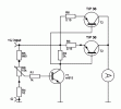
Voltage causes a current, not the other way around! So to make a device that provides a constant current no matter the load, we have to use negative feedback and convert the current flowing through our load into a voltage. Luckily, there is a very easy way to convert a current to a voltage which involves using a small ohm resistor (in our case, a 0.1-ohm resistor). The voltage across this resistor will be proportional to the current (thanks to V = IR) and using that, we can fix the current through the circuit. The voltage across the resistor is fed into the negative input of an op-amp and a fixed known voltage is fed into the positive terminal. The output of the op-amp is connected to the base of a power transistor (ignoring the Darlington pair) which controls how much current can flow through the circuit. The op-amp in this circuit (U1A) is in a closed loop because the negative input and output are connected together (through Q3) and so the op-amp will “attempt” to keep the + and – terminals at the same voltage potential.
The best way to see how this circuit works is an example:
We want to set our constant current source to 1 amp and we have connected a load of 1 ohm across the output. If 1 amp flows through the circuit, then we should expect to see a voltage of 0.1V across the 0.1-ohm resistor and so, therefore, we tune the potentiometer such that a voltage of 0.1V is fed into the positive terminal of U1A.
If the current going through the load is lower than 1 amp then the voltage across the 0.1 ohm resistor will be less than 0.1V and this is seen at the negative terminal at U1A. Because the positive terminal is larger than the negative terminal the op-amp will become more positive and therefore increase the conduction of Q3. This increase in conduction of Q3 allows more current to flow through the load and the 0.1-ohm resistor. If the current flowing through the resistor goes beyond 1 amp, then the voltage across the 0.1ohm resistor becomes greater than 0.1V. This means that the negative input to the op amp U1A becomes bigger than the positive input, and therefore the op-amp becomes more negative. This reduction in output voltage results in the conduction of Q3 being reduced and thus conducts less. This reduces the current flowing through the load and therefore the 0.1ohm resistor.
To help see what the current flowing through the load is, a voltage meter is connected to an amplifier (U1B). The job of the amplifier is to amplify the voltage across the 0.1ohm resistor to a readable level for a cheap LED digital display. D1 is used to prevent EMF spikes that may be created by loads from damaging the transistor Q3. The transistor Q3 should be in a TO-3 case with some form of heat dissipation for currents over 100mA and should have both a heatsink and an additional fan for current above 1A.
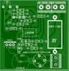
PCB layout for the constant current source
Required Materials
| Component | Schematic Reference | Quantity
| 10K Resistor | R1, R4 | 2
| 1K Resistor | R2, R5 | 2
| 0.1 Resistor (Power Metal Film) | R3 | 1
| 100nF Capacitor | C2, C3, C4 | 3
| 470uF Capacitor | C1 | 1
| 1N4148 Signal Diode | D1, D2 | 2
| LM358 | U1 | 1
| 8 DIP Socket | U1 | 1
| 100K Linear Potentiometer | RV1 | 1
| 2N3904 Transistor | Q1, Q2 | 2
| 2N3055 | Q3 | 1
| Digital LED Voltmeter | P4 | 1
Constructing the Constant Current Source
For this project, the circuit is powered by an old computer PSU (ATX) as these units can provide a substantial amount of current at low voltages. The constant current source currently does not have a dedicated case but instead uses an open style to demonstrate the construction. This circuit, despite outputting large currents, uses very low voltages (less than 12V) so this circuit is very safe (unlike mains-powered projects).
Circuit before wired up
Side view of test constant current source
Wiring to front panel
TO-3 mounting and fan assisted cooling