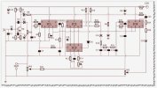
This is the schematic diagram of echo chamber circuit which will convert the input sound to have echo sound just like if you talking in the cave. This echo chamber circuit can be applied on any source of audio signal like microphone, mp3 player, radio, etc. The aims is smoothing the voices with echo.
The MN3005 is a world’s first 4096-stage long delay BBD, 8 times longer than S12-stage BBD manufactured by using a P-channel low noise silicon gate process.
Long signal delay time 205ms can be obtained at clock frequency 10KHz. S/N is 75dB. S/N has been improved by more than 20dB in comparting with 8~connected S12-stage BBD’s.
The MN3005 is suitably used for reverberation and echo effects in electronic musical instruments such as electronic organ, guitar amplifier and music synthesizer which need long delay time.The MN3101 is a CMOS LSI generating two phase clock signal of low output impedance to drive MN3000 series BBD. Built-in VGG power supply circuit for the MN3000 series BBD* provides most suitable VGG voltage for the BBD when the MN3101 is used with the same power source as BBD. Oscillation is abled by external resistors and capacitors, and also oscillation drive is possible by the separate excitation oscillation. Clock signal frequency is 1/2 of oscillation frequency.
Components List:
R1____________________________22K
R2, R3_________________________4K7
R4____________________________1K
R5____________________________82K
R6, R13, R19____________________47K
R7, R12, R23, R25________________120K
R8, R15, R16____________________100K
R9, R10________________________56K
R11, R12_______________________33K
R14___________________________15K
R17, R18_______________________5K6
R20, R21_______________________39K
R24, R26, R28___________________220k
R27, R29_______________________10K
C1, C18________________________2K2
C2____________________________1uF/16V
C3, C6, C7, C13__________________3,3uF/16V
C15, C16, C22, C23_______________3,3uF/16V
C4____________________________470pF
C5____________________________1K
C8, C9, C10_____________________3K3
C11, C12, C20___________________220pF
C14___________________________820pF
C17___________________________1K8
C19___________________________4K7
C21___________________________47K
C24___________________________100uF/16V
VR1___________________________200K
VR2___________________________10K Pot B
VR3___________________________20K
VR4___________________________100K
D1____________________________1N4148
D2____________________________9V Zener Diode
TR1___________________________C536
IC1, IC4_______________________AN6651
IC2___________________________MN3005
IC3,__________________________MN3101

