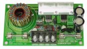
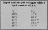
The converter raises a direct voltage to almost twice its level. It can deliver a current of up to 3A. Measurements with a load current of 2A are given in the table. The open-circuit output voltage is about 1-1.5 V higher.
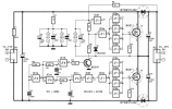
In the following description it is assumed that the input voltage to the circuit is 12 V and the output voltage 22 V. ICI1a, R2 and C5 form a rectangular-voltage generator. This signal is also available in inverted form at the output of IC1d. Network R2, C6, delays the output of ICI1a, so that the output of NAND gate ICI1b has a duty factor >0.5 (the negative half is shorter than the positive half). The same is true of the output of NAND gate ICI1c. (The input signal to this gate is delayed by R5-C7).
The output of ICI1c is inverted and buffered three times: in IC3f, IC3a, and the four paralleled gates IC3b-lC3e. It is then used to drive power FET T3.
The output of lC1b drives small-signal transistor T1. When this transistor is on, junction R6-R7 is pulled to 2 V without diode D1. However, IC2a needs an input signal of 11-22 V, since the supply voltage for this Inverter (and, of course, also for inverters IC2b-IC2e), as well as the collector voltage of T1 is already derived from the doubled output voltage. The negative supply voltage for this IC is therefore derived from the positive input voltage. Diode D1 ensures that the potential at the input of lC2a does not drop below 10.5 V
Transistors T2 and T3 conduct alternately. When T2 is on, C10 is charged to the level of the input signal via T3 and D3. When T2 is off and T3 is on, C9 is charged similarly. Capacitor C10 retains its charge, since D3 prevents its discharging. Since the two capacitors are in series, the output voltage is twice the input potential.
Owing to the multiple inversions of both signals following the delay networks, it is impossible for T2 and T3 to be switched on simultaneously. Capacitor C1 buffers the input signal, so that its loading is constant in spite of the varying current drawn by the circuit.
It is essential that D2, D3, T2, and T3 are well cooled. It is best to mount these components on a common heat sink. The bold lines in the schematic diagram represent heavy-duty wires that should be as short as possible, since they carry a current of 6 A.
A carefully constructed convertor should give an efficiency of 94% (at 22.2 V and 1.8 A).
Eklentiler
Son düzenleme:


