40w output amplıfıer wıth tda2030

Although there are a number of hybrid output modules on the market, very few of them combine compactness with reasonable price and good performance. One of these few is SGS's used in the present amplifier.
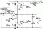
The design of the amplifier is straightforward: a power op-amp followed by two output transistors.
The audio signal is applied to the non-inverting input of power op-amp IC1 TDA2030 via socket K1 and capacitor C1. The supply current to the IC varies in accordance with the input signal. Consequently, there will be a similarly varying voltage drop across resistors R6, R7, R8, and R9 since these are in the supply lines to the op-amp.
As long as the current is lower than about 1A, the voltage drop across the resistors will be insufficient to switch on transistors T1 and T2. This means that outputs up to 2 W into 4 ohm are provided entirely by the op-amp. Once the output current exceeds a level of 1A, the transistors are on and contribute to the power output.
When the Input signal is small, there no quiescent current through the transistor, but there is through the op-amp. Crossover problems are thus obviated. Since the IC also provides thermal compensation, stability of the operating point is ensured.
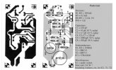
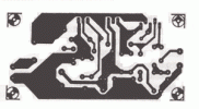
The supply voltage may lie between 12 V and an absolute maximum of 44 V. Construction of the amplifier on the printed-circuit board should be straightforward. The transistors as well as the IC must be fitted insulated on to a heat sink of about 2 k W. Use plenty of heat conducting paste. The supply line should be protected by a 3.15 A fuse. You can use BD911, BD912 for T1 and T2.


