This post meant to explains how to make a simple, cheap, small or compact yet extremely reliable smps or switching mode based 220V/120V mains to 5 volt dc operated cell phone battery charger circuit for high amperage batteries present in android and tabs these days.
Here we are going to use a simple IC having built in mosfet switching control circuit and also very reliable which allowes us to make a very compact but reliable circuit.
The TNY series of tiny switch ICs provide us with an option of making perhaps the smallest possible smps or switch mode based circuits with higher reliability. The tiny switch series includes the following ICs some of them are: TNY267P, TNY263, TNY264, TNY265, TNY266, TNY267, TNY268, TNY280.
The above ICs have an integrated built- in mosfet switching control circuit, there is also protection against over current and thermal overshoot, along with rugged voltage and current specifications provided. The IC comes in a DIP8 package that's exactly how a 555 is enclosed. The maximum tolerable voltage limit of the TNY series ICs is a massive 700V, that is a margin that id way too beyond our normal household AC specification. The operating frequency of this IC is at about 132kHz which is perfect for low power specification. The IC is specifically designed and built for implementing compact and reliable 120/220V mains operated SMPS flyback converter.
There may be a huge application for this switch mode power supply smps, it could be best used as a mains operated 5V cell phone charger circuit.
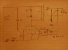
In this post cell phone battery charger design using the IC TY 267 can be visualized in the below shown diagram. The circuit can be understood as follows:
Circuit diagram

he mains input which can be anywhere between 100V and 280V AC is half wave rectified and filtered through shown 1N4007 diode and 10uF/400V input capacitor rectifier stage. Here the 10 ohm/1watt resistor is included to provide some sort of restriction against surge current occurrd during power switch ONs and also acts like a fuse in case of a catastrophic situation. The switching voltage is acquired via the BA159 diode at pin5 of the IC. The IC instantly locks into the specified 132kHz switching frequency when switched ON across the input winding of the switching ferrite transformer. The 180V zener diode protect the IC from peak switching voltages.
The above switching mode power supply generates the calculated stepped down low voltage across the output winding of the ferrite transformer. The BA159 diode at the output rectifies the 132kz pulsed DC while the 220uF capacitor filters the high frequency ripples to produce a clean ripple free DC.
Here the optocoupler acts like a tight feedback link between the output and the IC in order to ensure that the output never exceeds a certain predetermined or calculated voltage level at output terminals. This feedback limit is decided by the adjoining 4.7V zener diode, which ensures that the output stays well within the 5V range just suitable for charging any attached cell phone batteries.
How to wind the ferrite transformer used in above smps circuit
The shown ferrite transformer along with the IC forms the main component of the circuit, however due to its simple configuration winding this transformer is much easier compared to other mains operated cell phone battery charger circuit topologies. The input primary winding consists of around 140 turns of 36 SWG (standard wire guage), while the output secondary winding is made up of 8 turns of 27SWG (standard wire guage) super enameled copper wire turns. The core used can be a small E19 type ferrite core with bobbin having a central core area section measuring 4.5 by 4.5mm. The primary is wound first. After winding it, it must be covered with a layer of insulation before winding the 8 number of secondary turns on top of the primary layer. A copper or aluminum tape layer should be preferably included in between the primary and the secondary winding and a wire connected with this tape with the "cold" or Positive end of the primary winding (see the trafo in the figure), this provides guaranteed isolation between the winding as well as guards against interference issues.
To increase the output current simply increase the diameter of the secondary windings or wind parallel windings given that just join their ends.
To increase the output voltage just increase the secondary winding that's it.
Hoping you guys finds this circuit very interesting. Please ask any querry in comment section.
Here we are going to use a simple IC having built in mosfet switching control circuit and also very reliable which allowes us to make a very compact but reliable circuit.
The TNY series of tiny switch ICs provide us with an option of making perhaps the smallest possible smps or switch mode based circuits with higher reliability. The tiny switch series includes the following ICs some of them are: TNY267P, TNY263, TNY264, TNY265, TNY266, TNY267, TNY268, TNY280.
The above ICs have an integrated built- in mosfet switching control circuit, there is also protection against over current and thermal overshoot, along with rugged voltage and current specifications provided. The IC comes in a DIP8 package that's exactly how a 555 is enclosed. The maximum tolerable voltage limit of the TNY series ICs is a massive 700V, that is a margin that id way too beyond our normal household AC specification. The operating frequency of this IC is at about 132kHz which is perfect for low power specification. The IC is specifically designed and built for implementing compact and reliable 120/220V mains operated SMPS flyback converter.
There may be a huge application for this switch mode power supply smps, it could be best used as a mains operated 5V cell phone charger circuit.
In this post cell phone battery charger design using the IC TY 267 can be visualized in the below shown diagram. The circuit can be understood as follows:
Circuit diagram

he mains input which can be anywhere between 100V and 280V AC is half wave rectified and filtered through shown 1N4007 diode and 10uF/400V input capacitor rectifier stage. Here the 10 ohm/1watt resistor is included to provide some sort of restriction against surge current occurrd during power switch ONs and also acts like a fuse in case of a catastrophic situation. The switching voltage is acquired via the BA159 diode at pin5 of the IC. The IC instantly locks into the specified 132kHz switching frequency when switched ON across the input winding of the switching ferrite transformer. The 180V zener diode protect the IC from peak switching voltages.
The above switching mode power supply generates the calculated stepped down low voltage across the output winding of the ferrite transformer. The BA159 diode at the output rectifies the 132kz pulsed DC while the 220uF capacitor filters the high frequency ripples to produce a clean ripple free DC.
Here the optocoupler acts like a tight feedback link between the output and the IC in order to ensure that the output never exceeds a certain predetermined or calculated voltage level at output terminals. This feedback limit is decided by the adjoining 4.7V zener diode, which ensures that the output stays well within the 5V range just suitable for charging any attached cell phone batteries.
How to wind the ferrite transformer used in above smps circuit
The shown ferrite transformer along with the IC forms the main component of the circuit, however due to its simple configuration winding this transformer is much easier compared to other mains operated cell phone battery charger circuit topologies. The input primary winding consists of around 140 turns of 36 SWG (standard wire guage), while the output secondary winding is made up of 8 turns of 27SWG (standard wire guage) super enameled copper wire turns. The core used can be a small E19 type ferrite core with bobbin having a central core area section measuring 4.5 by 4.5mm. The primary is wound first. After winding it, it must be covered with a layer of insulation before winding the 8 number of secondary turns on top of the primary layer. A copper or aluminum tape layer should be preferably included in between the primary and the secondary winding and a wire connected with this tape with the "cold" or Positive end of the primary winding (see the trafo in the figure), this provides guaranteed isolation between the winding as well as guards against interference issues.
To increase the output current simply increase the diameter of the secondary windings or wind parallel windings given that just join their ends.
To increase the output voltage just increase the secondary winding that's it.
Hoping you guys finds this circuit very interesting. Please ask any querry in comment section.
