| The flyback dc-dc converter topology
results in significant cost and space savings
for multiple output power supplies with high
output voltage for power levels up to 100W.
Flyback topologies store and transfer energy
using a transformer, which due to physical
limitations can cause large voltage transient
spikes during the switching cycle. This article
outlines the design of dissipative voltage
suppression circuits (voltage snubbers) that can
be used to suppress these transients on both the
primary and secondary side.
The flyback topology
(Figure 1A) results in significant cost
and space savings for multiple output power
supplies with high output voltage for power
levels up to 100W. This topology uses a
transformer, which is essentially a coupled
inductor with multiple windings on the same
magnetic core. Flyback topologies operate by
storing energy in the transformer during the
power switch on-time and transferring this
energy to the output during the off-time. The
energy is stored in a non-magnetic gap in series
with the transformer core. In practice, the
multiple windings cannot all be equally well
coupled to the core because of the physical
separation between the windings. A small amount
of energy is also stored within and between
these windings. This energy is represented in
the circuit as a leakage inductance (Figure
1B).

Figure
1A. Basic topology of flyback circuit.

Figure
1B. Equivalent transformer model.
The flyback topology is attractive for
multiple output supplies because the output
voltages track one another with line and load
changes and because adding outputs to the system
does not require additional ICs. Despite its
advantages, the flyback has the disadvantage of
large transient voltage spikes at the drain of
the power switch and at the secondary rectifier.
These spikes are a function of the leakage
inductance in the flyback transformer. Snubbers
control the effects of the leakage inductance
and improve the reliability of the power supply.
Snubbers can be either passive or active
networks. Passive snubber network elements are
restricted to resistors, capacitors, inductors
and diodes. Passive snubbers can control either
voltage or current and may be either dissipative
or non-dissipative. If the energy in the snubber
is dissipated in a resistive element it is
classified as a dissipative snubber, but if the
energy is returned to the input or moved ahead
to the output it is classified as
non-dissipative. This application note provides
an overview of the different types of passive
dissipative voltage snubbers used, guidelines on
how they are designed, and their various
limitations. In particular, snubbers used to
reduce the stress on the switch and improve
efficiency in a flyback topology are discussed.
The first section enumerates the need for a
snubber on the primary side of a flyback
converter. The second section explains the need
for a snubber on the output side. This is
followed by a discussion of the various types of
dissipative voltage snubbers.
Primary Leakage Inductance and the MOSFET
SwitchThe primary leakage inductance
LLP in a flyback does not participate
in the primary to secondary energy transfer and
so has a negative impact on efficiency. Since
the leakage inductance does not find a path for
the current built up in it during the switch
on-time, it leads to a voltage spike at the
turn-off of the MOSFET and also delays the
transfer of power from the primary to the
secondary. The parasitic elements in the
transformer and the switch determine the
magnitude of this voltage spike. At high output
voltagesthe circuit parasitics become large
relative to the amount of output power
delivered.
The primary leakage inductance,
LLP, and the primary winding
capacitance in the transformer, CP,
and the output capacitance, COSS, of
the MOSFET form a parasitic LC network. The peak
voltage is given by:
VPEAK = IP ( (LLP/(CP+COSS)))
+ VIN + VOUT/N (LLP/(CP+COSS)))
+ VIN + VOUT/N
Where IP is the current level
circulating at the time the MOSFET turns OFF, N
is the ratio of secondary to primary turns,
VIN is the input voltage, and
VOUT is the output voltage.
The square root term in the above equation
represents the characteristic impedance of the
parasitic LC network. Note that the highest
voltage transient occurs when switching the
highest level of current. This voltage overshoot
may cause excessive power dissipation in the
MOSFET even if it is within safe operating
limits of the device and thus reduce the total
efficiency. Also, it may cause instability in
the loop due to (dv/dt) induced spurious turn-on
of the MOSFET as a result of the transient
voltage spike.
Secondary Leakage Inductance and the
Rectifier DiodeThe transformer secondary
leakage inductance may couple with the reverse
recovery current IREC of the output
rectifier diode to cause ringing when the diode
turns off. The transformer secondary leakage
inductance LLS and the capacitance
CD of the rectifier determine this
resonant frequency. The ringing may generate
significant radiated and conducted noise. There
is typically very little loss in the resonant
circuit so this network will cause many cycles
of ringing after the spike. The ringing can
therefore affect the current sense signal used
by the controller in a flyback configuration.
The overshoot caused by this ringing may exceed
the diode voltage rating and cause damage to the
diode. The maximum positive voltage across the
rectifier can be estimated as
VPEAK,S = IREC(LLS /CD) +
VIN  N N
The damping of the resonant circuit should be
optimized as excessive damping can also lead to
increased switching times and result in
increased losses.
A snubber could therefore be used to clamp
the voltage spike or damp the ringing to reduce
noise in the system or both. Depending on the
function performed by the snubber it can be
broadly classified into three categories:
- Rate-of-rise control snubber
- Voltage clamp snubber
- Damping snubber
Damping snubbers are dissipative by
definition. Rate-of-rise control snubbers and
voltage clamp snubbers may be dissipative or
non-dissipative. Non-dissipative snubbers are
generally resonant type snubbers. Snubbers can
also be classified as polarized or non-polarized
depending on whether energy moves in or out of
the snubber at either switching edge or at both.
The polarized snubber is not very good at
damping since it is not active during much of
the cycle. It usually provides rate-of-rise
control or clamping. Depending on whether the
parameter being controlled is voltage or current
these snubbers can be further classified as
voltage or current snubbers. Only dissipative
type voltage snubbers are discussed in this
application note.
RCD Voltage Snubber
This snubber is
applicable to rate-of-rise voltage control
and/or clamping. The presence of the diode in
the configuration makes this a polarized
snubber. The two possible configurations for
this resistor-capacitor-diode (RCD) snubber are
shown in Figure 2. The configuration
shown in Figure 2A can only act as a voltage
clamp. The variation shown in Figure 2B is
applicable to either rate-of-rise control or
clamping of the drain voltage of the switch.

Figure
2A. Voltage clamp snubber.

Figure
2B. Rate-of-rise voltage snubber.
RCD Clamp
In the clamp mode the
purpose of the snubber is to clamp the voltage
during turn-off at the drain of the MOSFET. The
parallel RC circuit may be returned to ground or
to a voltage other than ground (i.e., input
voltage if the drain can go above input voltage)
since this will reduce the power dissipation in
the resistor. The MOSFET switch itself will have
to sustain the peak power dissipation during
turn-off. The value of the capacitor,
CCLAMP, and resistor,
RCLAMP, is based on the energy stored
in the parasitic inductance, as this energy must
be discharged into the RC network during each
cycle. The voltage across the capacitor and
resistor sets the clamp voltage,
VCLAMP. The turn-off waveform at the
drain of the MOSFET switch is as shown in
Figure 3.

Figure
3. MOSFET turn-off waveforms with clamping.
This implies that the power dissipated in the
clamp at turn-off is
PCLAMP = (1/2) VCLAMP ICLAMP  t f t f
Where, f is the switching frequency.
However,
t = (LLP
IP)/(VCLAMP -
VOUT/N).
The power dissipated in the clamp is through
the resistor. Therefore
RCLAMP = [2 VCLAMP (VCLAMP -
VOUT/N)]/( LLP
IP2 f)
It is important to minimize the ripple,
Vripple, superimposed on
VCLAMP to keep the MOSFET drain
voltage close to the clamp voltage. The minimum
value for the capacitor, CCLAMP, is
therefore CCLAMP = VCLAMP/
(Vripple RCLAMP f).
The capacitor, CCLAMP, should have
a low ESR and low inductance to handle the high
peak currents during turn-off. The RC time
constant of the clamp should be chosen much
larger than the switching period of the MOSFET.
The series diode used in the clamp should be
able handle the peak currents and must be a fast
turn-on type.
The RC network may be replaced by a zener
diode that can handle the voltage rating and the
power dissipation. However, since the zener is
not a fast switching device a capacitor may
still be needed in parallel with the zener to
handle the high frequency currents. Note that
this snubber is not used in topologies with a
clamped inductive load since it does not reduce
ringing.
Rate-of-Rise Control RCD
Snubber
When the RCD snubber is used to
control the rate of voltage rise at the MOSFET
drain, the capacitor must be completely charged
and discharged during each cycle to be able to
control the rate-of-rise of the drain voltage.
The RC time constant of the snubber should,
therefore, be much smaller than the switching
period (consider the effect of duty cycle on
pulse width). Typically, the time constant
should be about 1/10th the switching
period. When the switch turns off, the inductor
current is diverted through the snubber diode to
charge the capacitor to the rail. At that time,
it is expected that the output rectifier will
turn on.
When the switch turns on, the snubber
capacitor will discharge through the snubber
resistor and the switch.
The capacitance value is obtained from
IP = C (VC/ tr)
Where VC = voltage across the
capacitor and tr = rise time of the
voltage
The resistor is then chosen based on the time
constant required. The RC time constant is much
smaller than the switching frequency and,
therefore, the power dissipated in the resistor
is independent of its value. The power
dissipation is determined by the value of the
capacitance and the switching frequency. Since
there is only one transition (discharge) through
the resistor, the power dissipation in the
resistor is given by P =
(CVC2f)/2.
Simple RC Snubber
This is probably
the most widely used snubber and is applicable
for both rate-of-rise control and damping. In
inductively clamped topologies, where there is
still some stray inductance, the RC snubber can
be used to reduce the peak power dissipation in
the switch by controlling the rate-of-rise of
drain voltage. The RC snubber, however, will
absorb energy during each voltage transition and
can reduce efficiency. Also, the RC snubber will
reduce the switching speed of the MOSFET switch.
Care must be used in choosing the value of R and
C to optimize the total performance. The main
application of a RC snubber is to damp parasitic
ringing in the circuit due to unclamped
inductance in configurations such as the flyback
converter. In these applications, the value of
the resistor must be close to the characteristic
impedance of the parasitic resonant circuit it
is intended to damp. Choose the snubber resistor
to be
R = (Lres/Cres)
Where Lres = parasitic inductance
causing the resonance, Cres =
parasitic capacitance causing the resonance.
The RC time constant of the snubber should be
small compared to the switching period but long
compared to the voltage rise time. The snubber
capacitance must be larger than the parasitic
resonance capacitance, but small enough to
minimize dissipation in the snubber resistor.
The snubber capacitance is generally chosen to
be at least 3 to 4 times the value of the
parasitic resonant capacitor. The power
dissipated can be estimated from the snubber
capacitance as
P = C
(VC)2 f
Where C is the snubber capacitance,
VC is the voltage across the snubber
capacitor, and f is the switching frequency.
It is very important to pay attention to
parasitics in the components used in the snubber
since these may render the snubber ineffective.
The diodes used in snubbers should be able to
handle large peak currents, but the average
current is relatively small. The PC board layout
may need to provide some heat sink area for
these diodes. Capacitors have series inductance
and this should be minimized to avoid
introduction of any unwanted resonance in the
circuit. Some electrostatic capacitors (ceramic
and polymer film) offer extremely low ESR and
ESL values. Capacitors can be paralleled to
reduce circuit inductance. Care must be
exercised in using this method. The series
inductance of a large capacitance is capable of
resonating with a small capacitance in parallel
with it and the resulting resonant circuit will
have a high Q.
The resistors used should have very low
inductance to avoid excessive overshoots and
ringing. Avoid using wirewound resistors. The
layout should not introduce stray inductance,
especially in high current paths. The
transformer used in flyback converters should be
designed to reduce leakage inductance and
minimize overshoot and ringing. The actual
design of the transformer is, however, beyond
the scope of this application note and will be
discussed elsewhere.
The switches in the circuit are usually the
most susceptible devices that need snubbing. The
switch is also in the input stage of the flyback
circuit. In practice, the best procedure is to
start from the input and proceed to the output
stage when introducing the snubbers into the
circuit. Once a node has been shown to need a
snubber, the purpose of the snubber should be
determined before selecting the type.
A flyback topology application circuit using
the MAX1856 is shown in Figure 4. This is
an example of using two snubber circuits for
different objectives. D3, C11 and R11 form a
clamp to limit the drain voltage and R5 with C10
forms a RC snubber to damp the ringing at the
secondary rectifier (D2). Comparing the
waveforms in Figure 5A and Figure
5B demonstrates the effect of the RC snubber
at the secondary rectifier.

Figure
4. Flyback application circuit using the
MAX1856.

Figure
5A. Voltage at the D2 rectifier cathode without
a snubber. (CH1= Voltage waveform at EXT/pin 8
of MAX1856; CH2= cathode of rectifier D2).
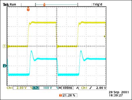
Figure
5B. Voltage at the D2 rectifier cathode with a
snubber (R5=150 ; C10=330 pF). (CH1= Voltage waveform
at EXT/pin 8 of MAX1856; CH2= cathode of
rectifier D2). ; C10=330 pF). (CH1= Voltage waveform
at EXT/pin 8 of MAX1856; CH2= cathode of
rectifier D2).
In conclusion, this application note has
discussed the use of passive voltage snubbers
with particular reference to flyback converter
topology. A properly snubbed circuit is more
efficient, more reliable and will perform well
over time, within temperature and production
tolerances. It is important to understand and
use the snubber circuits when it is necessary to
control switching voltage transients.
We Want Your
Feedback!
Love it? Hate it? Think it
could be better? Or just want to comment?
Please let us know—we act on customer
corrections and suggestions. Rate this page and provide
feedback.
Automatic
Updates
Would you like to be
automatically notified when new application
notes are published in your areas of interest?
Sign
up for EE-Mail.
| More Information |
|
APP 848: Nov 12, 2001
|
|
|
|
 Download, PDF
Format (140kB) Download, PDF
Format (140kB)
AN848, AN 848, APP848,
Appnote848, Appnote 848
| |